PS3 Hardware Questions (Extra USB Port?)

Technical discussion on the newly released and hard to find PS3.

Moderators: cheriff, emoon

Post Reply
User avatar
boxbuilder
Posts: 15
Joined: Sat Nov 17, 2007 3:13 pm

PS3 Hardware Questions (Extra USB Port?)

Post by boxbuilder »

Not quite sure where to put this, but here goes...

First the rant:
After speedtesting my usb harddrives and finding 15MB/s and 25MB/s dd to /dev/null speeds, I began looking at the motherboard pics to figure out why I wasn't getting 480Mb/s or 60MB/s from each of the 4 usb ports. After looking at the motherboard pictures at
http://media.ps3scene.com/images/PS3-motherboard-PAL/
I found that the 4 usb jacks all go to a splitter, and the ps3 only really has 1 usb port, I think the specs are misleading and am considering returning my system for a refund.

Now the questions:

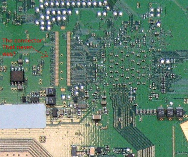
1.) While looking at the pictures, I counted 32 printed wires which do not go anywhere, they simply terminate.
16 come from the chip which sits downstream from the RSX (right and center in PS3_motherboard_8.jpg), 8 wires appear to come out of the cxr713120 (top right PS3_motherboard_7.jpg) and end below and to the right of the cell and near where f6301 is printed (seen in PS3_motherboard_8.jpg)
4 (2 pairs) come from the marvell ethernet controller
And the ones I'm most interested in: 4 (2 pairs) come from the south bridge, and terminate next to the Ethernet controller. I am interested in thiese because they come from the same place on the southbridge as the single USB line, and the wire widths and spacing are the same as with the SINGLE usb line.
Could these be usb? Is there a safe way to test? If I could get 3 480Mb/s lines out of the ps3, it may be worth keeping even though the specs are deceiving.

2.)How does the RSX read and write the XDRAM? there are no physical connections so I assume the cell helps out. Is this done at a hardware or firmware level? and most importantly, to what memory address can the RSX read/write? Cell ppu cache? registers? southbridge chip?

If anyone can shed some light on these topics, any help would be much appreciated. Also if anyone has pictures of the motherboards of the early ps3s with 2 Ethernet ports, please post the link

EDIT:

3.) WHERE DID THE RAM GO?

on the motherboard there are 4 XDR chips which are identified (by chipworks) as K4Y50164UC-JCB3 512Mb
that makes 2 gigs so far.
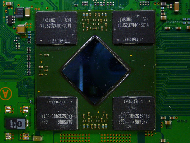
Chipworks also identifies 4 nec 0E128. If 128 is megabytes we are now up to 3 gig. In this picture http://pc.watch.impress.co.jp/docs/2006/1111/ps3_38.jpg
the inner heatsink was removed from the rsx chip revealing 4 samsung K4j523240C-sc14
A similer chip was identified here:
http://64.233.169.104/search?q=cache:kq ... =firefox-a
and it read as follows:
samsung 522
K4j523240C-BC12

1- K=Samsung Memory
2- 4=DRAM
3- J=GDDR3 SDRAM
4,5- 52= 512M, 8K/32 (Density and Refresh)
6,7- 32= x32 (Organization)
8- 2= 2 Banks
9- 4= LVTTL (3.3V, 3.3 V ) (Interface VDD, VDDQ)
**** things get interesting in this two, i can't read if is DC or 0C
but it's not in the samsung graphic memory nomenclature
Thies appear to be 4 more 512MB DRAM chips, bringing the grand total to 5 gigabytes of ram, a heahthy amount for a 64 bit processor.

Now why does linux only recognize 256MB of ram, and 256MB of video ram?

I can understand them using some ploys to trade volume for other benefits (speed? accuracy?) but only being able to address 10% of the memory is absurd.[/quote]
Last edited by boxbuilder on Mon Jul 28, 2008 10:59 am, edited 1 time in total.
jimparis
Posts: 1145
Joined: Fri Jun 10, 2005 4:21 am
Location: Boston

Re: PS3 Hardware Questions

Post by jimparis »

boxbuilder wrote:After speedtesting my usb harddrives and finding 15MB/s and 25MB/s dd to /dev/null speeds, I began looking at the motherboard pics to figure out why I wasn't getting 480Mb/s or 60MB/s from each of the 4 usb ports. After looking at the motherboard pictures at
http://media.ps3scene.com/images/PS3-motherboard-PAL/
I found that the 4 usb jacks all go to a splitter, and the ps3 only really has 1 usb port, I think the specs are misleading and am considering returning my system for a refund.
The specs say there are 4 USB ports, and there are. They are attached to the root hub, just like in a normal PC.

Have you checked your harddrives on another system? Only relatively new disks would be able to sustain 60MB/sec. And USB certainly carries a lot of overhead that would prevent you from ever reaching that speed anyway.
While looking at the pictures, I counted 32 printed wires which do not go anywhere, they simply terminate. ... Could these be usb? Is there a safe way to test?
I don't know how you can tell the difference between "terminate" and "go into a micro via" on those pictures, but even if those lines were connected to a supposed additional USB interface on the SCC, you're not going to be able to convince the hypervisor to expose that to otheros.
2.)How does the RSX read and write the XDRAM?
DMA operations through the southbridge, like you'd see on a normal PC architecture.
3.) WHERE DID THE RAM GO?
...
Thies appear to be 4 more 512MB DRAM chips, bringing the grand total to 5 gigabytes of ram, a heahthy amount for a 64 bit processor.
It's not gigabytes, it's gigabits. 4 gigabits = 512 megabytes.
only being able to address 10% of the memory is absurd.
so is wild speculation :)
User avatar
boxbuilder
Posts: 15
Joined: Sat Nov 17, 2007 3:13 pm

Post by boxbuilder »

Thank you for your reply,

megabits, of course!
meaning there is 256MB of XDR and 512MB of video ram (maybe some kind of page flipping scheme.)

I have never heard of a computer which squashed all of it's usb communications into one usb channel, using a usb hub chipset.

Testing my hard drive I discovered it must be conflicting with the sata->usb adapter, I had installed another drive with the same adapter in my pc and got a reported 70MB/s, I naively assumed that the bottleneck was on the usb end, and skipped testing it with this drive.

I am still interested in the unused wires. I'm not sure what you mean by "go into a micro via" but I uploaded a pic of the apparent ends of those wires.
http://bayimg.com/jajlpaaBp

Good point about the hypervisor, but I would think this would be one of few issues $ony would be willing to help out on, after all, it has almost no chance of being useful to load pirate games.
DMA operations through the southbridge, like you'd see on a normal PC architecture.
Where is this southbridge? in the pics I looked at, the RSX is connected only to the cell, and another chip which is not connected to any ram. Anyway I was asking specifically about the RSX blitting to a cache in the XDRAM the fast stuff which only appears to be connected to the cell chip.

Thank you again for your kind help, and I hope you don't mind my idle speculation (where did I leave that pipe? ;-)

-whatisaname?
User avatar
mc
Posts: 211
Joined: Wed Jan 12, 2005 7:32 am
Location: Linköping

Re: PS3 Hardware Questions

Post by mc »

jimparis wrote:The specs say there are 4 USB ports, and there are. They are attached to the root hub, just like in a normal PC.
That's not true, for the 60GB model at least. There are two USB channels, each with a 2 port root hub. But the 4 USB ports on the front are not connected directly to any root hub,
but to a stand-alone hub (GL852), which is then connected to the root hub of one of the channels.
See http://mc.pp.se/ps3/usb.xhtml.
Flying at a high speed
Having the courage
Getting over crisis
I rescue the people
User avatar
boxbuilder
Posts: 15
Joined: Sat Nov 17, 2007 3:13 pm

Post by boxbuilder »

Micro via = multilayer motherboard
Explains a lot, but reduces tracing wires to guesswork :(

After reading your page mc, I looked at the plugs for the usb/wifi board, and found four of the same types of wires which also appear to "terminate".

It's interesting that you found an unused port because there has been a picture kicked around the net of a white ps3 with usb ports in the back.
Image

One hypotheses is that the motherboard was supposed to be in the middle of the ps3, with a daughterboard with another usb hub, and an Ethernet router chip plugged in above, but when they actually started the thing up, it made so much heat that they needed to skip the daughterboard, and raise the motherboard to the top to allow for the monster cooling system below.

Do people think that they were actually trying to give us this many ports, or just blowing hot air?

And for my last question (for now)

What is This?
Image


Hope I inspired some thought...


EDIT:
Looking at the above picture indicates there is 1 set of two wires with a ground on either side (upper left,) these wires don't go anywhere on the front or back, so must be run through an inside layer, looks like the most likely place to find the forth usb.
The rest of that connector is 7 sets of 4 wires between grounds, 4 sets of 6, and 2 sets of 5, and a single next to the"usb".
Maybe Sony would give us a map of those connection points, it's easier than giving us RSX.
_______________________________________________________________
Vote Ron Paul for freedom!
watch http://video.google.com/videoplay?docid ... 9643041382
User avatar
mc
Posts: 211
Joined: Wed Jan 12, 2005 7:32 am
Location: Linköping

Post by mc »

The "white" (silver, actually) PS3 is the prototype which was shown at E3 2005. It wasn't
really working, but presumably the 6 USB ports did reflect some actual plans (which later
got scrapped) for how the final system should be. I expect cost was a bigger factor
than cooling in the reduction of the number of ports (not just USB, but also HDMI
and ethernet ports got cut down).
Flying at a high speed
Having the courage
Getting over crisis
I rescue the people
jimparis
Posts: 1145
Joined: Fri Jun 10, 2005 4:21 am
Location: Boston

Post by jimparis »

Aah, thanks for the correction mc, nice to know.
TheDoctor
Posts: 2
Joined: Sat Aug 16, 2008 10:21 am

Post by TheDoctor »

One thing to keep in mind is that the hard drive in the ps3s are SATA. Serial ATA ports are controlled by a similar chip on the ps3 as the USB root hub. If in fact you find what appears to be an "extra" usb controller, it is most likely the SATA controller chip.
Post Reply