
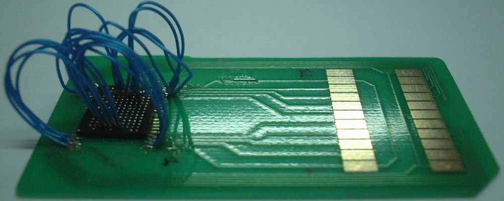
K5E5658HCM-D060 PSP NAND Flash Adaptor
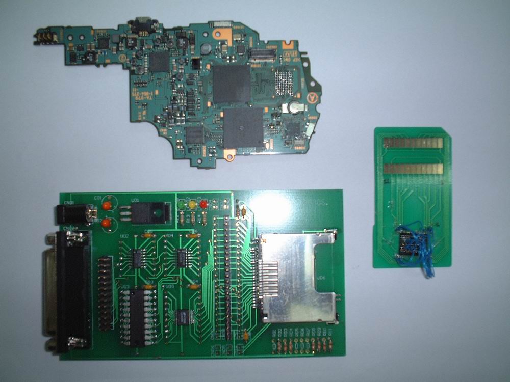
PSP MainBoard, NAND Flash Programer, PSP NAND Flash Adaptor
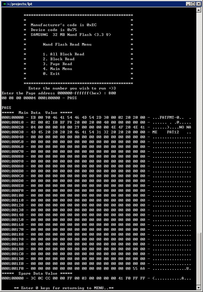
Read PSP NAND Flash DATA to PC

Actually, it may not be as bad as we think, with some hardware purchases:ryoko_no_usagi wrote:To hook it up in-circuit, one would have to find a way to keep the nand-interface in the CPU from hogging the bus. Probably by cutting the traces, which is...messy...
the "NAND Flash Programer" was build by meDibblah wrote:I should have thought of searching for this :)
http://cgi.ebay.co.uk/SMARTMEDIA-PARALL ... dZViewItem
will probably be the same hardware.....
Er, I think you misunderstood me. :) That's probably a nice kit for BGA rework, but it is a little overkill for hooking into the nand since all the traces are exposed on the top layer (luck or what?). Probably a lot easier (not to mention cheaper) to just solder wires onto them...Dibblah wrote:Actually, it may not be as bad as we think, with some hardware purchases:ryoko_no_usagi wrote:To hook it up in-circuit, one would have to find a way to keep the nand-interface in the CPU from hogging the bus. Probably by cutting the traces, which is...messy...
http://www.stencilsunlimited.com/bga_stencils.php
Then just install a "shim" that pulls out either side of the flash interface (to and from chip). Since you're not changing the different trace-lengths of anything important (it's just the flash lines - The others would need through-holed).
It's a lot of work for DIY, but with the right equipment, it looks easy.
True for the USB ones. But not the parallel - All of the smarts there pretty much have to be in the driver...0okm0000 wrote:the "NAND Flash Programer" was build by meDibblah wrote:I should have thought of searching for this :)
http://cgi.ebay.co.uk/SMARTMEDIA-PARALL ... dZViewItem
will probably be the same hardware.....
you can not use CardReader to read NandFlash SpareData & BadBlock
so you need to dev hardware by yourself
or buy the NandFlash devKit/Programer
Bet if you will keep reset low the CPU wont even try to do anything and all pins will be in high-z. So you can access Flash that time safely. Probably it possible to make some nail pad which will let you work with Flash chip right on PSP withou soldering :)It's no good if you have a conflict when you try to assert WE and the CPU want to deassert it for instance :)
Great...so where's the reset? :)KPOT0B wrote:Bet if you will keep reset low the CPU wont even try to do anything and all pins will be in high-z.It's no good if you have a conflict when you try to assert WE and the CPU want to deassert it for instance :)
It's a SpongeBob Squarepants ice-cream actually...sea_monster wrote: i would have to agree with Ryoko, the one there who is eating furry ice cream or something.
The traces aren't the biggest ever of course, but it's perfectly possible to graft wires onto them ;)sea_monster wrote: who cares about soldering to those traces, since those lines are not associated with the crazy fast ram. Problem is, have you SEEN those traces? I was pretty giddy about the via's that almost all the lines ran to. But that was based on photos. Upon seeing an actual board, everything is pretty intimidatingly small.
Yeah, they all look accessible. I'm too busy these days to work on this much,shifty wrote:I am finding it hard to believe that all flash traces are on the top
layer. Can someone confirm this? (zoomed, non-blurry photo would
help construction). Additionally, are Vcc and Vss also on top?
If you hook into the nand traces and don't power the CPU when you access the nand, the signals will attempt feed the CPU backwards, which is not so good.shifty wrote: Does anyone think we might be able to power the flash and r/w it with the rest of the PSP turned off? I suspect strongly that we can.
ryoko_no_usagi wrote:Did they rewrite the whole nand? I think some characteristics of the nand/psp might be stored in one place in the nand which means it might not be a good idea to blindly overwrite everything. According to Mathieulh, the official updater doesn't touch this area....
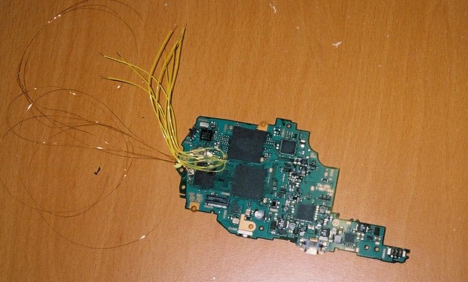
Wow ! That's what I call a real mess ! xDnem wrote:Mainboard mod for 'Titan Base', my attempt to interrupt flash line:
http://sec.pn.to/pw/?plugin=attach&pcmd ... efer=Bases